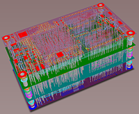
PCB stack-up is an important factor in determining the EMC performance of a product. A good stack-up can be very effective in reducing radiation from the loops on the PCB (differential-mode emission), as well as the cables attached to the board (common-mode emission). On the other hand, a poor stack-up can increase the radiation from both of these mechanisms considerably.

4 factors are important with respect to board stack-up considerations:
1. The number of layers,
2. The number and types of planes (power and/or ground) used,
3. The ordering or sequence of the layers, and
4. The spacing between the layers.

Usually not much consideration is given except as to the number of layers. In many cases the other three factors are of equal importance. Item number four is sometimes not even known by the PCB designer. In deciding on the number of layers, the following should be considered:
1. The number of signals to be routed and cost
2. Frequency
3. Will the product have to meet Class A or Class B emission requirements
4. Will the PCB be in a shielded or unshielded enclosure
5. The EMC engineering expertise of the design team
Often only the first item is considered. In reality all the items are of critical importance and should be considered equally. If an optimum design is to be achieved in the minimum amount of time and at the lowest cost, the last item can be especially important and should not be ignored.
Multi-layer boards using ground and/or power planes provide significant reduction in radiated emission over two layer PCBs. A rule of thumb, that is often used, is that a four-layer board will produce 15 dB less radiation than a two-layer board, all other factors being equal.Boards containing planes are much better than those without planesfor the following reasons:
1. They allow signals to be routed in a microstrip (or stripline) configuration. These configurations are controlled impedance transmission lines with much less radiation than the random traces used on a two-layer board.
2. The ground plane decreases the ground impedance (and therefore the ground noise) significantly.
Although two-layer boards have been used successfully in unshielded enclosures at 20 to 25 MHz, these cases are the exception rather than the rule. Above about ten or fifteen MHz, multi-layer boards should normally be considered.

When using multi-layer boards there are five objectives that you should try to achieve. They are:
1. A signal layer should always be adjacent to a plane.
2. Signal layers should be tightly coupled (close) to their adjacent planes.
3. Power and Ground planes should be closely coupled together.
4. High-speed signals should be routed on buried layers located between planes. In this way the planes can act as shields and contain the radiation from the high-speed traces.
5. Multiple ground planes are very advantageous, since they will lower the ground (reference plane) impedance of the board and reduce the common-mode radiation.
Often we are faced with the choice between close signal/plane coupling (objective #2) and close power plane/ground plane coupling (objective #3). With normal PCB construction techniques, there is not sufficient inter-plane capacitance between the adjacent power and ground planes to provide adequate decoupling below about 500 MHz. The decoupling, therefore, will have to be taken care of by other means and we should usually opt for tight coupling between the signal and the current return plane. The advantages of tight coupling between the signal (trace) layers and the current return planes will more than outweigh the disadvantage caused by the slight loss in interplane capacitance.
An eight-layer PCB board is the fewest number of layers that can be used to achieve all five of the above objectives. On four and six layer board some of the above objectives will have to be compromised. Under those conditions you will have to determine which objectives are the most important to the design at hand.
The above paragraph should not be construed to mean that you can't do a good EMC design on a four- or six-layer board, because you can. It only indicates that all the objectives cannot be met simultaneously and some compromise will be necessary. Since all the desired EMC objectives can be met with an eight-layer board, there is no reason for using more than eight layers other than to accommodate additional signal routing layers.

Another desirable objective, from a mechanical point of view, is to have the cross section of the board symmetrical (or balanced) in order to prevent warping. For example, on an eight-layer board if layer two is a plane, then layer seven should also be a plane. Therefore, all the configurations presented here use symmetrical, or balanced, construction. If a non-symmetrical, or unbalanced, construction is allowed additional stack-up configurations are possible.


 My Message
 Suggestions


Michele Perniola
2/2/2017 8:59:00 PM
Really appreciate your content.I hope you write again soon.