 My Message
 Suggestions


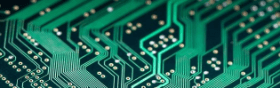
With pin pitches shrinking on FPGAs and other IC packages, many printed-circuit board (PCB) designers—like it or not—are forced to enter the realm of high-density interconnects (HDIs). In response to this trend, Cadence has announced the SPB 16.2 release of its Allegro and OrCAD families of PCB design flow. While the flow has offered constraint-driven design for some time, that capability is now coupled with new features aimed at HDIs.
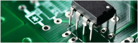
New technology introduced in Allegro PCB for HDI designs includes new objects, an extensive set of new rules for micro-vias, an enhanced via-transition use model, and changes to the entire PCB design flow to enable a comprehensive constraint-driven HDI design flow. Design partitioning has been enhanced with new capabilities for partitioning the design horizontally and adding soft boundaries to allow users to work in parallel more efficiently, further shortening the design cycle.
Designers can shorten their time to market and reduce development costs for high-frequency signals such as those found in PCI Express 2.0, Serial ATA II, and SAS II. Using Allegro PCB SI users can quickly and accurately simulate and validate for bit-error-rate compliance using new and advanced eye-mask capabilities and high-frequency field-solver technology. In addition, Allegro PCB SI provides simulation support for interoperable, multi-vendor IBIS 5.0 AMI-compliant transceivers.
With the layout-driven RF PCB design capability introduced in the new release, users can eliminate the need to manually update schematics for RF circuit elements added into the layout. Combined with an improved bi-directional integration with Agilent’s ADS environment, the Allegro PCB RF option allows users to shorten time to create mixed-signal digital-analog-RF designs.
The SPB 16.0 release made a significant investment in improving the ease of use of Allegro and OrCAD PCB Editor. The new release continues this emphasis on improving ease of use for all products in the Allegro family, from design creation tools in the front end to PCB layout tools in the back end.
OrCAD Capture boasts productivity and usability improvements including an updated graphical user interface (GUI), enhanced search capabilities, and new capability for designing in FPGAs. New FPGA design-in features include the ability to create split symbols, import, and export FPGA pin assignments for leading FPGA vendor tools, and ease-of-use improvements for supporting the ECO process for FPGAs.
Finally, engineers can specify and embed physical and spacing constraints for critical high-speed nets in the design to improve chances of first-time success while eliminating traditional error-prone verbal, e-mail, and spreadsheet-based communication. This can help shorten design cycles and eliminate unnecessary iterations between hardware designers and PCB layout designers.
SPB 16.2 will be available in Q4 2008; contact Cadence directly for pricing information. Users can see demos of Allegro PCB and IC packaging/SiP flows at the CDNLive! Silicon Valley conference in San Jose (Sept. 9-11). SPB 16.2 also will be demonstrated at the EMA booth at the PCB West in Santa Clara (Sept 14-19).


neil.edlin
1/22/2017 5:26:06 PM
I like checking your post and hope your update comes soon.